|
 |
|
|
Once a design is complete it must be manufactured or else it will remain just so much wallpaper. This process involves removing hierarchy by flattening the circuit, modifying the layout graphics for the manufacturing needs, making a template or mask for each layer, fabricating the actual circuit, and then packaging it for use. The set of synthesis tools to be discussed here is concerned with the layout modifications that must be done for this process.
When a circuit is fabricated, differences are introduced between the mask data and the true circuit. For example, contact cuts involve the removal of material from previous layers, and because of the nature of the chemicals used, more area gets removed than is indicated on the mask. In order to get the correct dimensions on the final artifact, the mask dimensions must be compensated, in this case by shrinking.
Compensation is highly process-dependent--much more so than design rules. For example, most MOS processes have design rules that prevent polysilicon lines from being closer together than they are wide, but one process will compensate polysilicon by shrinking the geometry, whereas another process will bloat it. One reason that the direction of compensation is so variable is that some masks are negative and some positive, so it is never clear whether a layer's creation is the result of etching away unwanted material or protecting what is wanted.
Shrinking on the final circuit indicates the need to bloat on the mask, which is called positive compensation. When the mask is to be shrunk, that is negative compensation. This compensation is typically performed immediately prior to mask creation and is therefore never displayed to the designer.
Positive compensation is quite simple: Every polygon is made larger by the specified amount. This is done by moving all coordinates away from the center of the polygon. When two polygons overlap because they have each grown, there may be no need to remove the redundancy. This is because the mask-generation process sorts all the polygons prior to writing them and can merge overlaps easily.
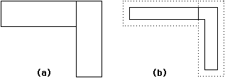
| Negative compensation is more difficult because two adjacent polygons that shrink will no longer adjoin. Polygon edges that border other polygons on the same layer therefore must not be shrunk. This requires the negative compensation process to spend much time exploring the neighborhood of each polygon. Once a common border is found, it may be necessary to break an edge into multiple edges in order to maintain connectivity while still shrinking (see Fig. 4.19). |
|
The only ameliorating aspect of negative compensation is that it may be possible, in special circumstances, to do it as easily as positive compensation. If, for example, the contact-cut layer is to be shrunk, then there is no fear about loss of adjacency, because no two contact-cut polygons ever connect. This special case is not uncommon and should be available in the compensation system to save time. It presupposes, however, that no other part of the design system has divided a single contact cut into multiple polygons. If this assumption cannot be made, then more rigorous compensation must be done.
Compensation is one of the "hidden" operations in IC layout because the designer does not think about it at all. Nevertheless, it is a crucial step that enables the finished chip to resemble the specified design.
There are special markings that must be placed on the masks of an integrated circuit. These markings are used for mask alignment, process checking, and wafer cutting. In general, they are placed on a mask after compensation because their specified dimensions are indicative of desired mask markings and not wafer markings.
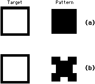
| Alignment marks are needed on every layer so that the masks can be properly registered with each other. Typically the first mask to be used has a series of empty target boxes on it. Each subsequent layer to be aligned will then have a pattern that fits into one of these boxes. Almost any pattern and target will do, but they should be designed so that they can be easily spotted on the masks and do not obscure each other during alignment. If there are uniform gaps in the pattern-target overlap, it will be easier to check visually for alignment errors (see Fig. 4.20). Also, these gaps will help if one or both of the masks is produced as a negative image because of process requirements. |
|
Maximum alignment accuracy is achieved by aligning all masks against the first one. This ensures that no masks are more than two alignment errors off from each other. In some cases, however, it is more important that a particular pair of masks align with each other than that they align with the overall wafer. In such cases, the set of masks will contain their own targets rather than use targets from the first layer. Decisions about which layers should be targeted against which other layers are generally made by process engineers, who best understand the important dependencies.
Another mark that is placed on a mask is a fiducial for gross alignment. These marks are simply crosses in the corners that can be quickly aligned. Generally, fiducials are placed on the masks by the mask-making shop and do not have to be specified explicitly.
Yet another marking that process engineers need is called critical dimensions; these are used to check and adjust the quality of the fabrication. Critical dimensions are sets of minimum-width marks on each layer, which are checked under a microscope as the wafer is manufactured. When the process parameters are adjusted to obtain the proper critical dimensions, the rest of the chip is likely to turn out well.
Critical dimensions, like alignment marks, belong in a distinctive place on the chip that will be easy to find under a microscope. Rather than being hidden in some unused area on the chip, these marks belong in a corner, outside of the active circuitry. This extra chip space does not increase the probability of a defect that can damage circuit performance. In fact, having some extra space outside the active circuitry will help spread the individual chips on a wafer, which will make it easier to cut the wafer without damaging the chips.
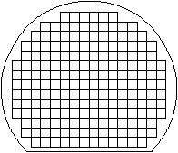
| Wafer cutting, sometimes called scribing or sawing, is the subject of another piece of mask graphics that a design system must handle. Scribe lanes are fairly wide lines that run horizontally and vertically across the wafer. They typically form a regular grid inside the round area of the wafer and do not extend to the edges (see Fig. 4.21). A CAD system that prepares wafer masks does not need to replicate the chip in each location on the wafer. Rather, it is sufficient to specify a complete chip with its scribe lanes and then indicate where on the wafer this chip will appear. Typically there are also test circuits that are inserted in a few of the chip locations to check different vicinities of the wafer. |
|
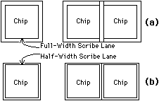
| One decision that must be made in placing scribe lanes is whether to put a full- or half-width lane around each chip. With a full-width lane, the chips will have to overlap on the wafer by one-half of the scribe-lane width in order to fit properly (see Fig. 4.22). This overlap is somewhat confusing to specify and costs extra mask-making time since all scribe lanes are then drawn twice. With a half-width scribe-lane border, each chip can abut its neighbors exactly and build a clean wafer. The disadvantage of half-width scribe lanes is that chips on the edge of the wafer will be damaged during scribing unless the other half of the outside scribe lane is specified explicitly. These edge chips are sometimes useless anyway since fabrication quality is best near the prime center area of the wafer. Another problem with half-width scribe lanes is that the test chips may not have any scribe lanes, to allow them to fit in any wafer scheme. This means that the four chips adjoining each test chip will also lack full scribe edges. |
|
The process engineer specifies exactly which layers should appear in the scribe lanes. In addition, a certain minimum spacing between the active circuitry and the scribe lane must be maintained. As a final consideration, the distance between scribe-lane centers must not be irregular because scribing machines are less accurate than are mask-making machines. For example, the scribe-lane spacing may have to be a multiple of 5 mils (five thousandths of an inch). All these details are process-dependent.
The last piece of graphics that a CAD system should be able to place on a layout is text. All designers document their circuitry by spelling out messages. This text will include the circuit name, different letters for each layer, and any other message of interest. This text not only is useful for documentation purposes but also serves to verify the correct side of a mask during fabrication. Instructions to the processing staff often include an indication as to whether the mask should be placed "right reading" or "wrong reading" according to how the text appears [Hon and Sequin]. This is easier to determine than some arbitrary symbol location or shape.
Mask graphics is a significant layout task that CAD systems often overlook; rather than providing these symbols, the designer is often forced to produce them manually. A good system not only will provide text and graphics but will help with the entire mask-preparation process by understanding what is necessary and where it should be placed.
|
Previous |  |
Table of Contents | Next | |
Static Free Software |  |