Copyright Michael Karbo and ELI Aps., Denmark, Europe.
Chapter 28. The cache
In the previous chapter, I described two aspects of the ongoing development of new CPUs increased clock frequencies and the increasing number of transistors being used. Now it is time to look at a very different yet related technology the processors connection to the RAM, and the use of the L1 and L2 caches.
Speed conflict
The CPU works internally at very high clock frequencies (like 3200 MHz), and no RAM can keep up with these.
The most common RAM speeds are between 266 and 533 MHz. And these are just a fraction of the CPUs working speed. So there is a great chasm between the machine (the CPU) which slaves away at perhaps 3200 MHz, and the conveyor belt, which might only work at 333 MHz, and which has to ship the data to and from the RAM. These two subsystems are simply poorly matched to each other.
If nothing could be done about this problem, there would be no reason to develop faster CPUs. If the CPU had to wait for a bus, which worked at one sixth of its speed, the CPU would be idle five sixths of the time. And that would be pure waste.
The solution is to insert small, intermediate stores of high-speed RAM. These buffers (cache RAM) provide a much more efficient transition between the fast CPU and the slow RAM. Cache RAM operates at higher clock frequencies than normal RAM. Data can therefore be read more quickly from the cache.
Data is constantly being moved
The cache delivers its data to the CPU registers. These are tiny storage units which are placed right inside the processor core, and they are the absolute fastest RAM there is. The size and number of the registers is designed very specifically for each type of CPU.

Figure 68. Cache RAM is much faster than normal RAM.
The CPU can move data in different sized packets, such as bytes (8 bits), words (16 bits), dwords (32 bits) or blocks (larger groups of bits), and this often involves the registers. The different data packets are constantly moving back and forth:
The cache stores are a central bridge between the RAM and the registers which exchange data with the processors execution units.
The optimal situation is if the CPU is able to constantly work and fully utilize all clock ticks. This would mean that the registers would have to always be able to fetch the data which the execution units require. But this it not the reality, as the CPU typically only utilizes 35% of its clock ticks. However, without a cache, this utilization would be even lower.
Bottlenecks
CPU caches are a remedy against a very specific set of bottleneck problems. There are lots of bottlenecks in the PC transitions between fast and slower systems, where the fast device has to wait before it can deliver or receive its data. These bottle necks can have a very detrimental effect on the PCs total performance, so they must be minimised.
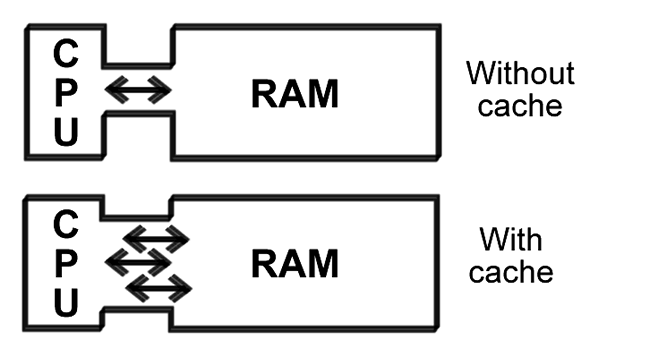
Figure 69. A cache increases the CPUs capacity to fetch the right data from RAM.
The absolute worst bottleneck exists between the CPU and RAM. It is here that we have the heaviest data traffic, and it is in this area that PC manufacturers are expending a lot of energy on new development. Every new generation of CPU brings improvements relating to the front side bus.
The CPUs cache is intelligent, so that it can reduce the data traffic on the front side bus. The cache controller constantly monitors the CPUs work, and always tries to read in precisely the data the CPU needs. When it is successful, this is called a cache hit. When the cache does not contain the desired data, this is called a cache miss.
Two levels of cache
The idea behind cache is that it should function as a near store of fast RAM. A store which the CPU can always be supplied from.
In practise there are always at least two close stores. They are called Level 1, Level 2, and (if applicable) Level 3 cache. Some processors (like the Intel Itanium) have three levels of cache, but these are only used for very special server applications. In standard PCs we find processors with L1 and L2 cache.
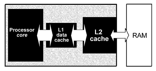
Figure 70. The cache system tries to ensure that relevant data is constantly being fetched from RAM, so that the CPU (ideally) never has to wait for data.
L1 cache
Level 1 cache is built into the actual processor core. It is a piece of RAM, typically 8, 16, 20, 32, 64 or 128 Kbytes, which operates at the same clock frequency as the rest of the CPU. Thus you could say the L1 cache is part of the processor.
L1 cache is normally divided into two sections, one for data and one for instructions. For example, an Athlon processor may have a 32 KB data cache and a 32 KB instruction cache. If the cache is common for both data and instructions, it is called a unified cache.
L2 cache
The level 2 cache is normally much bigger (and unified), such as 256, 512 or 1024 KB. The purpose of the L2 cache is to constantly read in slightly larger quantities of data from RAM, so that these are available to the L1 cache.
In the earlier processor generations, the L2 cache was placed outside the chip: either on the motherboard (as in the original Pentium processors), or on a special module together with the CPU (as in the first Pentium IIs).
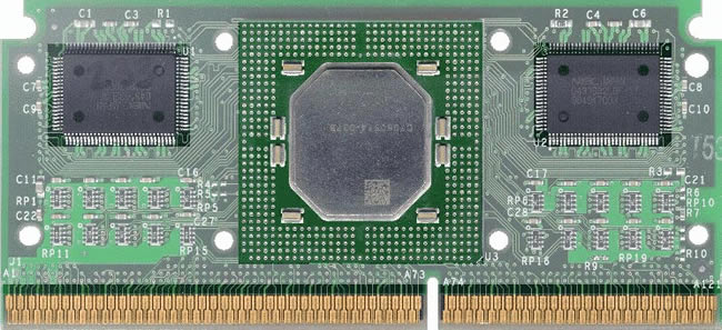
Figure 71. An old Pentium II module. The CPU is mounted on a rectangular printed circuit board, together with the L2 cache, which is two chips here. The whole module is installed in a socket on the motherboard. But this design is no longer used.
As process technology has developed, it has become possible to make room for the L2 cache inside the actual processor chip. Thus the L2 cache has been integrated and that makes it function much better in relation to the L1 cache and the processor core.
The L2 cache is not as fast as the L1 cache, but it is still much faster than normal RAM.
|
CPU |
L2 cache |
|
Pentium, K5, K6 |
External, on the motherboard |
|
Pentium Pro |
Internal, in the CPU |
|
Pentium II, Athlon |
External, in a module |
|
Celeron (1st generation) |
None |
|
Celeron
(later gen.), |
Internal, in the CPU |
Figure 72. It has only been during the last few CPU generations that the level 2 cache has found its place, integrated into the actual CPU.
Traditionally the L2 cache is connected to the front side bus. Through it, it connects to the chipsets north bridge and RAM:
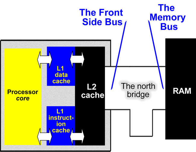
Figure 73. The way the processor uses the L1 and L2 cache has crucial significance for its utilisation of the high clock frequencies.
The level 2 cache takes up a lot of the chips die, as millions of transistors are needed to make a large cache. The integrated cache is made using SRAM (static RAM), as opposed to normal RAM which is dynamic (DRAM).
While DRAM can be made using one transistor per bit (plus a capacitor), it costs 6 transistors (or more) to make one bit of SRAM. Thus 256 KB of L2 cache would require more than 12 million transistors. Thus it has only been since fine process technology (such as 0.13 and 0.09 microns) was developed that it became feasible to integrate a large L2 cache into the actual CPU. In Fig. 66 on page 27, the number of transistors includes the CPUs integrated cache.
Powerful bus
The bus between the L1 and L2 cache is presumably THE place in the processor architecture which has the greatest need for high bandwidth. We can calculate the theoretical maximum bandwidth by multiplying the bus width by the clock frequency. Here are some examples:
|
CPU |
Bus |
Clock |
Theoretical bandwidth |
|
Intel Pentium III |
64 bits |
1400 MHz |
11.2 GB/sek. |
|
AMD
|
64 bits |
2167 MHz |
17.3 GB/sek. |
|
AMD Athlon 64 |
64 bits |
2200 MHz |
17,6 GB/sek. |
|
AMD Athlon 64 FX |
128 bits |
2200 MHz |
35,2 GB/sek. |
|
Intel Pentium 4 |
256 bits |
3200 MHz |
102 GB/sek. |
Figure 74. Theoretical calculations of the bandwidth between the L1 and L2 cache.
Different systems
There are a number of different ways of using caches. Both Intel and AMD have saved on L2 cache in some series, in order to make cheaper products. But there is no doubt, that the better the cache both L1 and L2 the more efficient the CPU will be and the higher its performance.
AMD have settled on a fairly large L1 cache of 128 KB, while Intel continue to use relatively small (but efficient) L1 caches.
On the other hand, Intel uses a 256 bit wide bus on the inside edge of the L2 cache in the Pentium 4, while AMD only has a 64-bit bus (see Fig. 74).

Figure 75. Competing CPUs with very different designs.
AMD uses exclusive caches in all their CPUs. That means that the same data cant be present in both caches at the same time, and that is a clear advantage. Its not like that at Intel.
However, the Pentium 4 has a more advanced cache design with Execution Trace Cache making up 12 KB of the 20 KB Level 1 cache. This instruction cache works with coded instructions, as described on page 35
|
CPU |
L1 cache |
L2 cache |
|
Athlon XP |
128 KB |
256 KB |
|
Athlon XP+ |
128 KB |
512 KB |
|
Pentium 4 (I) |
20 KB |
256 KB |
|
Pentium 4 (II, Northwood) |
20 KB |
512 KB |
|
Athlon 64 |
128 KB |
512 KB |
|
Athlon 64 FX |
128 KB |
1024 KB |
|
Pentium 4 (III, Prescott) |
28 KB |
1024 KB |
Figure 76. The most common processors and their caches.
Latency
A very important aspect of all RAM cache included is latency. All RAM storage has a certain latency, which means that a certain number of clock ticks (cycles) must pass between, for example, two reads. L1 cache has less latency than L2; which is why it is so efficient.
When the cache is bypassed to read directly from RAM, the latency is many times greater. In Fig. 77 the number of wasted clock ticks are shown for various CPUs. Note that when the processor core has to fetch data from the actual RAM (when both L1 and L2 have failed), it costs around 150 clock ticks. This situation is called stalling and needs to be avoided.
Note that the Pentium 4 has a much smaller L1 cache than the Athlon XP, but it is significantly faster. It simply takes fewer clock ticks (cycles) to fetch data:
|
Latency |
Pentium II |
Athlon |
Pentium 4 |
|
L1 cache: |
3 cycles |
3 cycles |
2 cycles |
|
L2 cache: |
18 cycles |
6 cycles |
5 cycles |
Figure 77. Latency leads to wasted clock ticks; the fewer there are of these, the faster the processor will appear to be.
Intelligent data prefetch
In CPUs like the Pentium 4 and Athlon XP, a handful of support mechanisms are also used which work in parallel with the cache. These include:
A hardware auto data prefetch unit, which attempts to guess which data should be read into the cache. This device monitors the instructions being processed and predicts what data the next job will need.
Related to this is the Translation Look-aside Buffer, which is also a kind of cache. It contains information which constantly supports the supply of data to the L1 cache, and this buffer is also being optimised in new processor designs. Both systems contribute to improved exploitation of the limited bandwidth in the memory system.
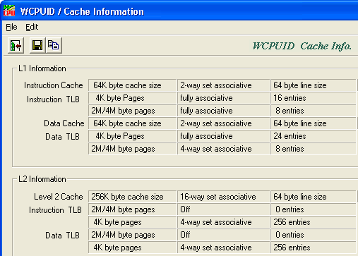
Figure 78. The WCPUID program reports on cache in an Athlon processor.
Conclusion
L1 and L2 cache are important components in modern processor design. The cache is crucial for the utilisation of the high clock frequencies which modern process technology allows. Modern L1 caches are extremely effective. In about 96-98% of cases, the processor can find the data and instructions it needs in the cache. In the future, we can expect to keep seeing CPUs with larger L2 caches and more advanced memory management. As this is the way forward if we want to achieve more effective utilisation of the CPUs clock ticks. Here is a concrete example:
In January 2002 Intel released a new version of their top processor, the Pentium 4 (with the codename, Northwood). The clock frequency had been increased by 10%, so one might expect a 10% improvement in performance. But because the integrated L2 cache was also doubled from 256 to 512 KB, the gain was found to be all of 30%.
|
CPU |
L2 cache |
Clock freq. |
Improvement |
|
Intel
Pentium 4 |
256 KB |
2000 MHz |
|
|
Intel
Pentium 4 |
512 KB |
2200 MHz |
+30% |
Figure 79. Because of the larger L2 cache, performance increased significantly.
In 2002 AMD updated the Athlon
processor with the new Barton core. Here the L2 cache was also doubled from
256 to 512 KB in some models. In 2004 Intel came with the
Xeon for servers
Intel produces special server models of their Pentium III and Pentium 4 processors. These are called Xeon, and are characterised by very large L2 caches. In an Intel Xeon the 2 MB L2 cache uses 149,000,000 transistors.
|
Xeon processors are incredibly expensive (about Euro 4,000 for the top models), so they have never achieved widespread distribution. They are used in high-end servers, in which the CPU only accounts for a small part of the total price. |
|
Otherwise, Intels 64 bit server CPU, the Itanium. The processor is supplied in modules which include 4 MB L3 cache of 300 million transistors.
Multiprocessors
Several Xeon processors can be installed on the same motherboard, using special chipsets. By connecting 2, 4 or even 8 processors together, you can build a very powerful computer.
These MP (Multiprocessor) machines are typically used as servers, but can also be used as powerful workstations, for example, to perform demanding 3D graphics and animation tasks. AMD has the Opteron processors, which are server-versions of the Athlon 64. Not all software can make use of the PCs extra processors; the programs have to be designed to do so. For example, there are professional versions of Windows NT, 2000 and XP, which support the use of several processors in one PC.
See also the discussion of Hyper Threading which allows a Pentium 4 processor to appear as an MP system. Both Intel and AMD also works on dual-core processors.