
Chapter 3
FULL-CUSTOM MASK LAYOUT DESIGN
![[previous]](../left.gif)
![[Table of Contents]](../toc.gif)
![[next]](../right.gif)

![[previous]](../left.gif)
![[Table of Contents]](../toc.gif)
![[next]](../right.gif)
In this chapter, the basic mask layout design guidelines for CMOS logic gates will be presented. The design of physical layout is very tightly linked to overall circuit performance (area, speed, power dissipation) since the physical structure directly determines the transconductances of the transistors, the parasitic capacitances and resistances, and obviously, the silicon area which is used for a certain function. On the other hand, the detailed mask layout of logic gates requires a very intensive and time-consuming design effort, which is justifiable only in special circumstances where the area and/or the performance of the circuit must be optimized under very tight constraints. Therefore, automated layout generation (e.g., standard cells + computer-aided placement and routing) is typically preferred for the design of most digital VLSI circuits. In order to judge the physical constraints and limitations, however, the VLSI designer must also have a good understanding of the physical mask layout process.
Mask layout drawings must strictly conform to a set of layout design rules as described in Chapter 2, therefore, we will start this chapter with the review of a complete design rule set. The design of a simple CMOS inverter will be presented step-by-step, in order to show the influence of various design rules on the mask structure and on the dimensions. Also, we will introduce the concept of stick diagrams, which can be used very effectively to simplify the overall topology of layout in the early design phases. With the help of stick diagrams, the designer can have a good understanding of the topological constraints, and quickly test several possibilities for the optimum layout without actually drawing a complete mask diagram.
The physical (mask layout) design of CMOS logic gates is an iterative process which starts with the circuit topology (to realize the desired logic function) and the initial sizing of the transistors (to realize the desired performance specifications). At this point, the designer can only estimate the total parasitic load at the output node, based on the fan-out, the number of devices, and the expected length of the interconnection lines. If the logic gate contains more than 4-6 transistors, the topological graph representation and the Euler-path method allow the designer to determine the optimum ordering of the transistors. A simple stick diagram layout can now be drawn, showing the locations of the transistors, the local interconnections between the transistors and the locations of the contacts.
After a topologically feasible layout is found, the mask layers are drawn (using a layout editor tool) according to the layout design rules. This procedure may require several small iterations in order to accommodate all design rules, but the basic topology should not change very significantly. Following the final DRC (Design Rule Check), a circuit extraction procedure is performed on the finished layout to determine the actual transistor sizes, and more importantly, the parasitic capacitances at each node. The result of the extraction step is usually a detailed
![[Zoom]](../zoom.gif)
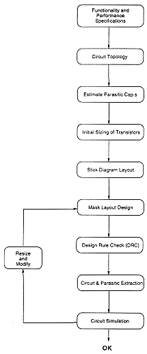
SPICE input file, which is automatically generated by the extraction tool. Now, the actual performance of the circuit can be determined by performing a SPICE simulation, using the extracted net-list. If the simulated circuit performance (e.g., transient response times or power dissipation) do not match the desired specifications, the layout must be modified and the whole process must be repeated. The layout modifications are usually concentrated on the (W/L) ratios of the transistors (transistor re-sizing), since the width-to-length ratios of the transistors determine the device transconductance and the parasitic source/drain capacitances. The designer may also decide to change parts or all of the circuit topology in order to reduce the parasitics. The flow diagram of this iterative process is shown in Fig. 3.1.
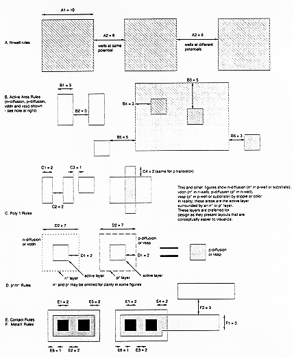
As already discussed in Chapter 2, each mask layout design must conform to a set of layout design rules, which dictate the geometrical constraints imposed upon the mask layers by the technology and by the fabrication process. The layout designer must follow these rules in order to guarantee a certain yield for the finished product, i.e., a certain ratio of acceptable chips out of a fabrication batch. A design which violates some of the layout design rules may still result in a functional chip, but the yield is expected to be lower because of random process variations.
The design rules below are given in terms of scaleable lambda-rules. Note that while the concept of scaleable design rules is very convenient for defining a technology-independent mask layout and for memorizing the basic constraints, most of the rules do not scale linearly, especially for sub-micron technologies. This fact is illustrated in the right column, where a representative rule set is given in real micron dimensions. A simple comparison with the lambda- based rules shows that there are significant differences. Therefore, lambda-based design rules are simply not useful for sub-micron CMOS technologies.
![[Zoom]](../zoom.gif)
![[Zoom]](../zoom.gif)
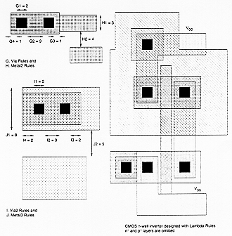
In the following, the mask layout design of a CMOS inverter will be examined step-by-step. The circuit consists of one nMOS and one pMOS transistor, therefore, one would assume that the layout topology is relatively simple. Yet, we will see that there exist quite a number of different design possibilities even for this very simple circuit.
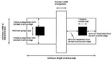
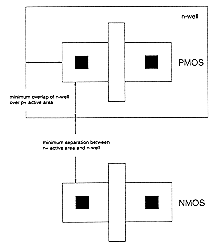
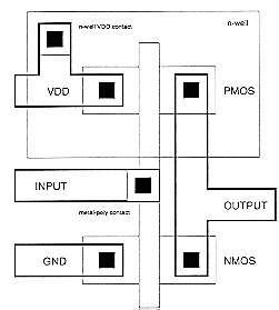
First, we need to create the individual transistors according to the design rules. Assume that we attempt to design the inverter with minimum-size transistors. The width of the active area is then determined by the minimum diffusion contact size (which is necessary for source and drain connections) and the minimum separation from diffusion contact to both active area edges. The width of the polysilicon line over the active area (which is the gate of the transistor) is typically taken as the minimum poly width (Fig. 3.3). Then, the overall length of the active area is simply determined by the following sum: (minimum poly width) + 2 x (minimum poly-to- contact spacing) + 2 x (minimum spacing from contact to active area edge). The pMOS transistor must be placed in an n-well region, and the minimum size of the n- well is dictated by the pMOS active area and the minimum n-well overlap over n+. The distance between the nMOS and the pMOS transistor is determined by the minimum separation between the n+ active area and the n-well (Fig. 3.4). The polysilicon gates of the nMOS and the pMOS transistors are usually aligned. The final step in the mask layout is the local interconnections in metal, for the output node and for the VDD and GND contacts (Fig. 3.5). Notice that in order to be biased properly, the n-well region must also have a VDD contact.
![[Zoom]](../zoom.gif)
![[Zoom]](../zoom.gif)
![[Zoom]](../zoom.gif)
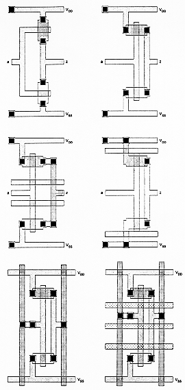
The inital phase of layout design can be simplified significantly by the use of stick diagrams - or so-called symbolic layouts. Here, the detailed layout design rules are simply neglected and the main features (active areas, polysilicon lines, metal lines) are represented by constant width rectangles or simple sticks. The purpose of the stick diagram is to provide the designer a good understanding of the topological constraints, and to quickly test several possibilities for the optimum layout without actually drawing a complete mask diagram. In the following, we will examine a series of stick diagrams which show different layout options for the CMOS inverter circuit.
The first two stick diagram layouts shown in Fig. 3.6 are the two most basic inverter configurations, with different alignments of the transistors. In some cases, other signals must be routed over the inverter. For instance, if one or two metal lines have to be passed through the middle of the cell from left to right, horizontal metal straps can be used to access the drain terminals of the transistors, which in turn connect to a vertical Metal-2 line. Metal-1 can now be used to route the signals passing through the inverter. Alternatively, the diffusion areas of both transistors may be used for extending the power and ground connections. This makes the inverter transistors transparent to horizontal metal lines which may pass over.
The addition of a second metal layer allows more interconnect freedom. The second- level metal can be used for power and ground supply lines, or alternatively, it may be used to vertically strap the input and the output signals. The final layout example in Fig. 3.6 shows one possibility of using a third metal layer, which is utilized for routing three signals on top.
![[Zoom]](../zoom.gif)
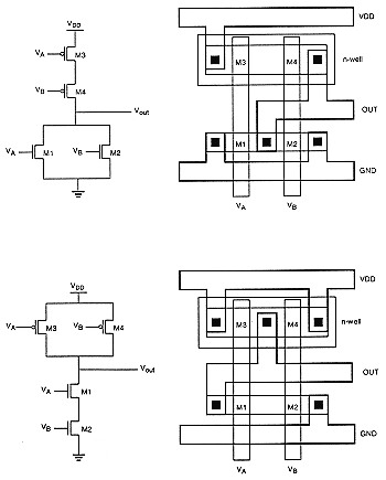
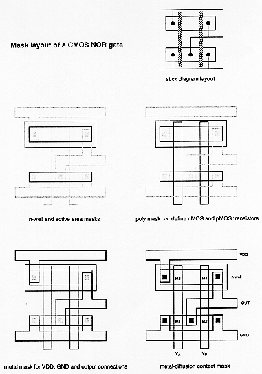
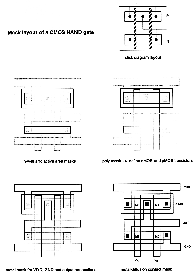
The mask layout designs of CMOS NAND and NOR gates follow the general principles examined earlier for the CMOS inverter layout. Figure 3.7 shows the sample layouts of a two- input NOR gate and a two-input NAND gate, using single-layer polysilicon and single-layer metal. Here, the p-type diffusion area for the pMOS transistors and the n-type diffusion area for the nMOS transistors are aligned in parallel to allow simple routing of the gate signals with two parallel polysilicon lines running vertically. Also notice that the two mask layouts show a very strong symmetry, due to the fact that the NAND and the NOR gate are have a symmetrical circuit topology. Finally, Figs 3.8 and 3.9 show the major steps of the mask layout design for both gates, starting from the stick diagram and progressively defining the mask layers.
![[Zoom]](../zoom.gif)
![[Zoom]](../zoom.gif)
![[Zoom]](../zoom.gif)
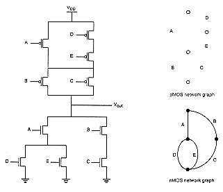
The realization of complex Boolean functions (which may include several input variables and several product terms) typically requires a series-parallel network of nMOS transistors which constitute the so-called pull-down net, and a corresponding dual network of pMOS transistors which constitute the pull-up net. Figure 3.10 shows the circuit diagram and the corresponding network graphs of a complex CMOS logic gate. Once the network topology of the nMOS pull- down network is known, the pull-up network of pMOS transistors can easily be constructed by using the dual-graph concept.
![[Zoom]](../zoom.gif)
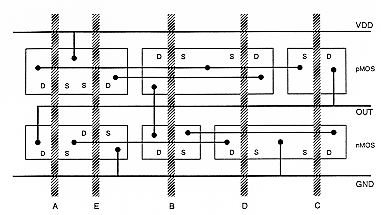
Now, we will investigate the problem of constructing a minimum-area layout for the complex CMOS logic gate. Figure 3.11 shows the stick-diagram layout of a �first-attempt�, using an arbitrary ordering of the polysilicon gate columns. Note that in this case, the separation between the polysilicon columns must be sufficiently wide to allow for two metal-diffusion contacts on both sides and one diffusion-diffusion separation. This certainly consumes a considerable amount of extra silicon area.
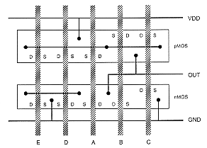
If we can minimize the number of active-area breaks both for the nMOS and for the pMOS transistors, the separation between the polysilicon gate columns can be made smaller. This, in turn, will reduce the overall horizontal dimension and the overall circuit layout area. The number of active-area breaks can be minimized by changing the ordering of the polysilicon columns, i.e., by changing the ordering of the transistors.
![[Zoom]](../zoom.gif)
A simple method for finding the optimum gate ordering is the Euler-path method: Simply find a Euler path in the pull-down network graph and a Euler path in the pull-up network graph with the identical ordering of input labels, i.e., find a common Euler path for both graphs. The Euler path is defined as an uninterrupted path that traverses each edge (branch) of the graph exactly once. Figure 3.12 shows the construction of a common Euler path for both graphs in our example.
![[Zoom]](../zoom.gif)
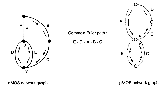
It is seen that there is a common sequence (E-D-A-B-C) in both graphs. The polysilicon gate columns can be arranged according to this sequence, which results in uninterrupted active areas for nMOS as well as for pMOS transistors. The stick diagram of the new layout is shown in Fig. 3.13. In this case, the separation between two neighboring poly columns must allow only for one metal-diffusion contact. The advantages of this new layout are more compact (smaller) layout area, simple routing of signals, and correspondingly, smaller parasitic capacitance.
![[Zoom]](../zoom.gif)
It may not always be possible to construct a complete Euler path both in the pull-down and in the pull-up network. In that case, the best strategy is to find sub-Euler-paths in both graphs, which should be as long as possible. This approach attempts to maximize the number of transistors which can be placed in a single, uninterrupted active area.
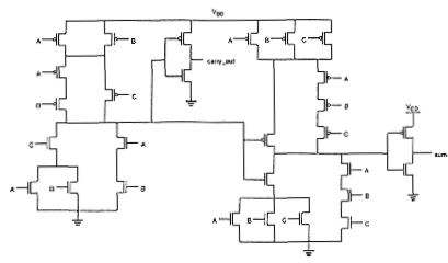
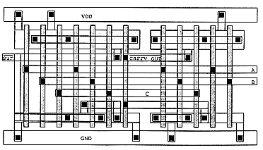
Finally, Fig. 3.14 shows the circuit diagram of a CMOS one-bit full adder. The circuit has three inputs, and two outputs, sum and carry_out. The corresponding mask layout of this circuit is given in Fig. 3.15. All input and output signals have been arranged in vertical polysilicon columns. Notice that both the sum-circuit and the carry-circuit have been realized using one uninterrupted active area each.
![[Zoom]](../zoom.gif)
![[Zoom]](../zoom.gif)
This chapter edited by Y. Leblebici