
Chapter 5
CLOCK SIGNALS AND SYSTEM TIMING
![[previous]](../left.gif)
![[Table of Contents]](../toc.gif)
![[next]](../right.gif)

![[previous]](../left.gif)
![[Table of Contents]](../toc.gif)
![[next]](../right.gif)
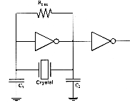
Clock signals are the heartbeats of digital systems. Hence, the stability of clock signals is highly important. Ideally, clock signals should have minimum rise and fall times, specified duty cycles, and zero skew. In reality, clock signals have nonzero skews and noticeable rise and fall times; duty cycles can also vary. In fact, as much as 10% of a machine cycle time is expended to allow realistic clock skews in large computer systems. The problem is no less serious in VLSI chip design. A simple technique for on-chip generation of a primary clock signal would be to use a ring oscillator as shown in Fig. 5.1. Such a clock circuit has been used in low-end microprocessor chips.
![[Zoom]](../zoom.gif)

However, the generated clock signal can be quite process-dependent and unstable. As a result, separate clock chips which use crystal oscillators have been used for high- performance VLSI chip families. Figure 5.2 shows the circuit schematic of a Pierce crystal oscillator with good frequency stability. This circuit is a near series-resonant circuit in which the crystal sees a low load impedance across its terminals. Series resonance exists in the crystal but its internal series resistance largely the determines the oscillation frequency. In its equivalent circuit model, the crystal can be represented as a series RLC circuit; thus, the higher the series resistance, the lower the oscillation frequency. The external load at the terminals of the crystal also has a considerable effect on the frequency and the frequency stability. The inverter across the crystal provides the necessary voltage differential, and the external inverter provides the amplification to drive clock loads. Note that the oscillator circuit presented here is by no means a typical example of the state-of-the-art; design of high-frequency, high-quality clock oscillators is a formidable task, which is beyond the scope of this section.
![[Zoom]](../zoom.gif)
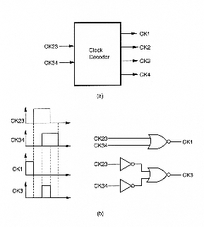
Usually a VLSI chip receives one or more primary clock signals from an external clock chip and, in turn, generates necessary derivatives for its internal use. It is often necessary to use two non-overlapping clock signals. The logical product of such two clock signals should be zero at all times. Figure 5.3 shows a simple circuit that generates CK-1 and CK-2 from the original clock signal CK. Figure 5.4 shows a clock decoder circuit that takes in the primary clock signals and generates four phase signals.
![[Zoom]](../zoom.gif)

![[Zoom]](../zoom.gif)
![[Zoom]](../zoom.gif)
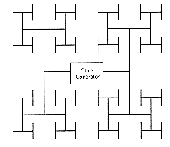
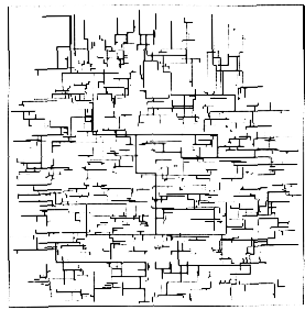
The reduction of clock skews, which are caused by the differences in clock arrival times and changes in clock waveforms due to variations in load conditions, is a major concern in high-speed VLSI design. In addition to uniform clock distribution (H-tree) networks and local skew balancing, a number of new computer-aided design techniques have been developed to automatically generate the layout of an optimum clock distribution network with zero skew. Figure 5.6 shows a zero-skew clock routing network that was constructed based on estimated routing parasitics.
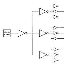
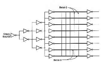
Regardless of the exact geometry of the clock distribution network, the clock signals must be buffered in multiple stages as shown in Fig. 5.7 to handle the high fan-out loads. It is also essential that every buffer stage drives the same number of fan-out gates so that the clock delays are always balanced. In the configuration shown in Fig. 5.8 (used in the DEC Alpha chip designs), the interconnect wires are cross- connected with vertical metal straps in a mesh pattern, in order to keep the clock signals in phase across the entire chip.
So far we have seen the needs for having equal interconnect lengths and extensive buffering in order to distribute clock signals with minimal skews and healthy signal waveforms. In practice, designers must spend significant time and effort to tune the transistor sizes in buffers (inverters) and also the widths of interconnects. Widening the interconnection wires decreases the series resistance, but at the cost of increasing the parasitic resistance.
![[Zoom]](../zoom.gif)
![[Zoom]](../zoom.gif)
![[Zoom]](../zoom.gif)
The following points should always be considered carefully in digital system design, but especially for successful high-speed VLSI design:
Ideal duty cycle of a clock signal is 50%, and the signal can travel farther in a chain of inverting buffers with ideal duty cycle. The duty cycle of a clock signal can be improved, i.e., made closer to 50%, by using feedback based on the voltage average.
To prevent reflection in the interconnection network, the rise time and the fall time of the clock signal should not be reduced excessively.
The load capacitance should be reduced as much as possible, by reducing the fan-out, the interconnection lengths and the gate capacitances.
The characterictic impedance of the clock distribution line should be reduced by using properly increased (w/h)-ratios (the ratio of the line width to vertical separation distance of the line from the substrate).
Inductive loads can be used to partially cancel the effects of parasitic capacitance of a clock receiver (matching network).
Adequate separation should be maintained between high-speed clock lines in order to prevent cross-talk. Also, placing a power or ground rail between two high-speed lines can be an effective measure.
This chapter edited by Y. Leblebici