|
 |
|
|
Regardless of the level of abstraction chosen for simulation, a number of key issues must be addressed. Some form of input is required, and the content may change with level of abstraction. Input includes a specification of the circuit or system to be simulated, information about the implementation technology (for example, characteristics of the particular CMOS process used), and logic or voltage values to apply to inputs. The basic simulation process uses this information to determine the values on a set of outputs after some amount of simulated time has passed. Finally, some means of displaying the results of the simulation must be incorporated in the simulator.
One of the tasks described in Chapter 5 was node extraction, which is the process of identifying circuit elements and their connectivity from a geometric representation of the layout. This information, along with some underlying information about the technology used to implement the circuit, is used by circuit- and logic-level simulators to determine a circuit's behavior. Circuit-level simulators require additional information regarding the capacitance of structures so that delays may be accurately calculated. It is the node extractor's job to calculate this additional information from the circuit layout (see the later section, Delay Modeling).
Gate-level simulators require a schematic of the design, expressed as standard logic gates connected by wires. Functional- and behavioral-level simulators operate on input that often closely resembles standard programming languages, with the behavior of a particular box given in a subroutinelike construct. In functional-level simulators, connectivity may be explicitly shown by wires carrying signals between functional units, or implicitly shown by functional units calling (in the manner of subroutines) other functional units with parameters. In behavioral-level simulators, connectivity is usually shown implicitly by call structure.
As each type of simulator requires a different type of design specification, maintaining consistency between the several representations of the design is a major problem in design-aid systems. Most systems leave the problem of maintaining consistent representations (that is, making sure that the geometric representation of a circuit does indeed match the functional description) up to the human user. Others attempt to maintain consistency automatically. Automatic schemes have been the most successful at the lower levels of abstraction; for example, for automatically compiling geometric layout from a gate-level schematic.
Simulation results can be useful in verifying the correctness of a design before implementation, as well as for diagnosing implementations of a design. Most designs are sufficiently complex that it is not possible to try all combinations of inputs systematically and to verify that the resulting behavior is correct. A much narrower range of tests needs to be provided as input to the simulator. Test inputs are used to specify the set of values that should be applied to a set of inputs at certain times during the simulation. Test inputs can be represented by a list of three-tuples, where each tuple consists of (input value time). Input is the location in the circuit that will be set to the logic value or voltage given by value at the time specified.
It is a nontrivial task to determine a set of test inputs that will sufficiently test a design. Most often test inputs are generated by hand by someone who is familiar with the design. Hand generation of test inputs has the advantage of exploiting a human's knowledge of the tricky or critical sections of the design. Of course, it is quite common for a human to miss or to test incompletely part of a design, particularly when the human is the same person who created the design.
So that human bias and error can be minimized in such situations, a good deal of research has gone into finding algorithms that can be systematically applied to a design in order to find errors. One example is the D-algorithm [Roth]. The D-algorithm was originally designed to test gate-level combinational logic designs, but other people have extended the algorithm (see, for example, [Jain and Agrawal] for an application to switch-level simulations).
Given a device that contains combinational logic with some set of inputs and some set of outputs, the goal of the D-algorithm is to find an assignment of input values that will allow the detection of a particular internal fault by examining the output values. In the D-algorithm, the existence of two machines-the "good machine" and the "faulty machine"-is hypothesized. The good machine works perfectly, whereas the faulty machine has some specific internal input stuck at a particular logic value (say, an input to an AND gate stuck at zero). The existence of the error causes a discrepancy between the behaviors of the good machine and the faulty machine for some values of inputs. The D-algorithm provides a means of systematically assigning input values so that this discrepancy is driven to an output, where it may be observed and thus detected. In other words, the D-algorithm provides a test input that is applied to a design. The output values are compared to the expected output values and any discrepancy indicates the presence of the particular internal fault that the test input was specifically designed to find (see [Miczo] for a good tutorial introduction to the D-algorithm as well as an overview of several other commonly used testing techniques).
The method by which a simulator handles time can intimately affect its performance. There are two primary methods of handling time; sometimes hybrid techniques that combine the two methods are used.
The first method runs the simulation as a series of fixed-length time steps. These incremental-time simulators advance the simulation clock a fixed amount of time, then calculate the values for all of the nodes in the design at the end of the time step. The time step is usually controllable by the user and is selected so that the finest-grain events of interest are not missed. Sometimes, circuit-level simulators use a variable time step that is controlled by the convergence properties of the equations.
The second method views the simulation as a series of events, where an event is a change to a node. A time-ordered priority queue of events is kept; when the simulator is running it processes events in the following way:
In both methods the calculation of a new value for a node can be quite expensive, depending on the accuracy desired. Typically, the calculation involves iteration until the nodes of interest do not change between successive iterations.
Each method has advantages and disadvantages. Incremental-time algorithms are relatively simple to implement and offer explicit control of the time grain of the simulation. Unfortunately, there may be long periods in the simulation during which few nodes change, yet the incremental-time method continues the expensive process of checking many nodes. In its simplest form, the incremental-time method often processes nodes that do not or cannot change from the previous time step to the current one. Various schemes have been developed to identify nodes or subcircuits that are inactive and therefore do not need to be recalculated. Event-driven algorithms attempt to avoid this problem by doing work only when something actually changes; their chief disadvantage is that they inherently have a variable time step and therefore may process many fine-grain events that are of no importance.
It is worth noting that most simulators have no built-in notion of time. The essential property is that time is a nondecreasing sequence of numbers. The relation of simulation-time units to real-time units is implicitly determined by the user when the component behaviors are specified. For example, in a gate-level simulation, it is convenient to give delays in units of nanoseconds rather than 0.000000001 seconds. In a switch-level simulation, units of basic inverter delay might be appropriate.
There are primarily two types of delay that are of concern to circuit designers: delay through "active components" and delay through wires. The exact definition of active component varies with the level of simulation--it might be a single transistor for a switch-level simulation, or it might be an entire ALU in a functional simulation.
Circuit-level simulators inherently calculate active-component and wire delay, since they are normally taken into account in the equations that are solved. For efficiency, logic-level simulators often assume a simplified model of delay, perhaps using a unit delay through active components and assuming zero delay through wires.
Many variations are possible. For example a functional simulator might use a table of delays for various functional blocks. The table could be based on actual observed delays for off-the-shelf components, if appropriate. Another class of simulator, called timing simulators [Terman; Chawla, Gummel, and Kozak], fits just above circuit-level simulators. Timing simulators use relatively complex (compared to most logic-level simulators) delay models combined with the simplification provided in assuming a fixed set of logic levels. For example, RSIM [Terman] uses a linear model of transistors to determine delay and final logic values for each node. The model takes into account the capacitance at each node and the drive capabilities, and is carefully tuned for each technology so that accurate results are obtained.
In cases in which a simple delay model, such as a unit-delay or table-driven approach, is used, the simulator needs only the connectivity of the circuit and the type of each node. However, much of the value of simulation lies in the ability to determine circuit delays accurately. When this detail is required, a more complex delay model is used.
These delay models approximate the fine-grain behavior of nodes and wires. The time that it takes a wire to change state, say from near 0 volts to near 5 volts, is determined by the resistance R and capacitance C of the wire. The delay depends exponentially on the product RC (for a more detailed explanation, see [Mead and Conway]). Thus, the simulator must be given the resistance and capacitance of each node and wire, in addition to device type and connectivity information.
The RC information is calculated in the node-extraction phase of design analysis. Consider a wire made of polysilicon in a MOS technology. The resistance of the wire is determined by its volume (= length × width × depth) and the resistance of the polysilicon. Since the resistance of the material and the depth of the wires is fixed for a particular implementation process, the node extractor need only calculate the length and width of the wire and multiply by a constant in order to determine its resistance. Similarly, the capacitance of the wire depends on its area, its separation from the underlying substrate, and the permittivity of the insulator that separates it from the substrate. The separation distance and the permittivity are fixed for the implementation process, and therefore the capacitance can be determined from the length and width of the wire [C = (permittivity × length × width) / separation].
Often this simple delay model suffices for approximating timing behavior. In cases for which it does not, more accurate calculation of resistance and capacitance can be performed and more complex delay equations used [Glasser and Dobberpuhl]. Nonplanar technologies such as bipolar may also require complex calculations to determine the resistance and capacitance of nodes and wires. As usual, the cost is time.
The choice of device model affects the accuracy and the speed of the simulation. The most accurate device models, often used by circuit-level simulators, are analytical and require an iterated solution to a set of equations. This type of model provides a close approximation to the analog behavior of the device, but requires a great deal of computation time.
Logic-level simulators often use simple table-driven models; for example, the behavior of a gate can be stored in a simple truth table and its output can be looked up once the inputs are known. Device delay can be assumed to be a single time unit, or can be calculated from a delay model that takes the actual device geometry into account.
The efficiency of table-driven models can be used in simulators that use multiple logic states by augmenting the truth tables with terms for each undefined or transition state.
As advancing technology allows more devices to be placed on a chip, it becomes increasingly difficult to dissipate the heat generated. In high-density, high-speed technologies, the exotic physical packaging required to remove heat can easily double the price of a system and can lead to attendant problems, for example in connecting to circuit boards for debugging. Thus, designers are often interested in the amount of power that their chips consume.
In nMOS designs, most of the power is consumed in depletion loads that are pulled low. As outlined in Chapter 5, a static estimation of power consumption can be made by determining how many loads can be pulled down. This may be needlessly pessimistic, since it is unlikely that all of the loads are pulled down simultaneously. Dynamic analysis can be used to provide a more accurate estimate of power dissipation, and can also take into account the actual switching frequencies.
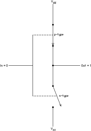
| In CMOS designs, depletion loads are not needed, since both n- and p-type transistors are available. As shown in the CMOS inverter of Fig. 6.4, when the input is zero the n-type transistor is off, and it can be easily seen that when the input is one the p-type transistor is off. This means that when the circuit is stable with input at zero or one, there is always one transistor that is off and hence no connection between Vdd and Vss. The only power dissipated is from leakage currents, which are typically small. |
|
When the input makes a relatively rapid transition from zero to one, the p-type transistor turns off while the n-type transistor turns on. Until they finish switching, Vss is connected to Vdd through a changing resistance (the two transistors in series), and so some power is dissipated. In addition, power is consumed in charging whatever capacitance is connected to the output. As shown in [Weste and Eshraghian], the power (P) consumed during these transitions is given by:
The total power is the sum of the power consumed while stable and the power consumed while switching. Once again, dynamic analysis can provide a more accurate estimate than can static analysis since the actual switching frequencies are known.
The output of simulators is at least a textual listing containing the values present on the monitored nodes as a function of time. This type of output has several significant disadvantages:
The next step up in output is exemplified in Fig. 6.1, where a rough graphical approximation to the waveforms is provided. The recent proliferation of graphics workstations enables simulation output to be presented in near-analog form, which makes comprehending the results much easier. Integration of the simulator results with the design-entry system further allows nodes to be graphically pinpointed.
|
Previous |  |
Table of Contents | Next | |
Static Free Software |  |